Hideki Hirayama教授:深紫外光电器件的现状与展望
在过去的二十年中,基于AlGaN的材料和器件发展迅速,但为了实现高性能AlGaN基光电器件,仍需要对其结构和工艺进行进一步的优化和改进,主要集中在三个方面:1. 降低AlGaN材料的缺陷密度。2. 提高器件结构的光提取效率。3. 实现AlGaN材料的高效P型掺杂。
为了解决上述问题,研究人员也做出了许多努力。为了在蓝宝石衬底上生长高质量的AlGaN材料,研究人员使用了多种方法来生长高质量的AlN薄膜,例如脉冲生长法、插入低温缓冲层或二维材料如石墨烯以及图案化蓝宝石衬底上的外延横向过生长技术。同时,在提高DUV-LED的p型层的透射率并减少外延层的自吸收的基础上,采用了图案衬底、表面粗糙化等技术可以进一步改善UV-LED的LEE和EQE。此外,对AlGaN的p掺杂研究还囊括了常见的均匀Mg掺杂,Mg-δ掺杂,超晶格掺杂,共掺杂,极化诱导掺杂等。就目前来看,虽然DUV-LED取得了一定的进展,但与基于GaN的蓝光和绿光LED相比,EQE仍然差强人意,未来将通过提高AlGaN的质量和p型掺杂以及优化AlGaN/AlN MQW的参数来实现高效的AlGaN基DUV-LED。与此同时,基于AlGaN的UV-LD的开发正在朝着更短的波长和更低的阈值电压发展。但是,要实现此类高性能LD,同样要进一步提高AlGaN质量和加强对p型掺杂的改进,同时还需要合适的LD结构设计以提高器件效率,低缺陷密度AlN体单晶衬底上同质外延为实现高性能LD的制造提供了一种有效途径。
在2019年第12期出版的《半导体学报》中,日本理化学研究所Hideki Hirayama教授撰写了Comments and Opinions 文章《Research status and prospects of deep ultraviolet devices》,综述了深紫外光电器件当前面临的机遇与挑战,展望了其未来发展的方向。
Ultraviolet (UV) radiation, which is an important component of solar radiation, can be divided into three bands, comprising the UV-A band (320–400 nm), the UV-B band (280–320 nm), and the UV-C band (100–280 nm). UV radiation affects not only the survival and continuing development of humankind, but also has a variety of important applications, including high-resolution light sources, phototherapy, disinfection, sterilization, deodorization, organic decomposition, photo catalysis, gas sensing, optical dialysis dosage monitoring, and the identification of hazardous biological agents[1].
UV light-emitting devices
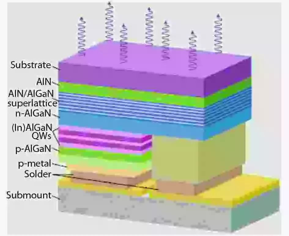
Taking the advantages of AlGaN materials of the direct wide bandgap character, great progress has been made in UV optoelectronic active devices, such as light-emitting diodes (LEDs) and laser diodes (LDs). Compared with traditional solid-state light sources, AlGaN-based UV-LEDs (Fig. 1) have numerous advantages, including short wavelength operation, small size, compact structure, operational stability, high efficiency, low power consumption, low operating voltage, environmental friendliness, and long lifetimes, which make them suitable for application in the UV radiation field[2-4]. Over the past two decades, AlGaN-based materials and devices experienced rapid development. Deep ultraviolet AlGaN-based LEDs with improved efficiency of 20.3% (at 275 nm) have been produced.

Figure 1. Schematic illustration of the DUV-LEDs structure.
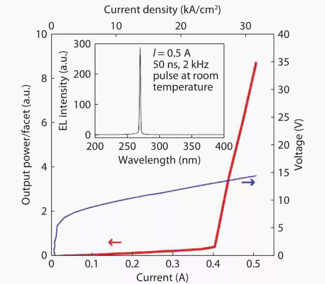
AlGaN-based UV-LDs with their unique high spatial and temporal coherence properties have many merits, including high light beam quality, high power density, and high modulation speeds, which can be widely used in applications of precision laser processing, high-density data storage, nanopattern-type photolithography, medical diagnostics, disinfection, biochemical technology, gas sensing, and materials science[5, 6]. Recently, Zhang et al. presented a deep-ultraviolet semiconductor laser diode that operates under current injection at room temperature and at a very short wavelength. The laser structure was grown on the (0001) face of a single-crystal aluminum nitride substrate. The measured lasing wavelength was 271.8 nm with a pulsed duration of 50 ns and a repetition frequency of 2 kHz (Fig. 2)[7].

Figure 2. I–V and edge emission I–L characteristics of the measured UV-C LD. The inset figure shows the edge emission spectrum at 0.5 A forward current[7].
Problems of UV light-emitting devices
In order to realize high-performance devices, further optimization and improvement of structure and manufacturing are required, mainly focusing on three aspects: reducing the defect density of AlGaN materials, improving the light extraction efficiency of device structures and achieving high-efficiency P-type doping of AlGaN materials.
(1) Poor-quality of AlGaN material
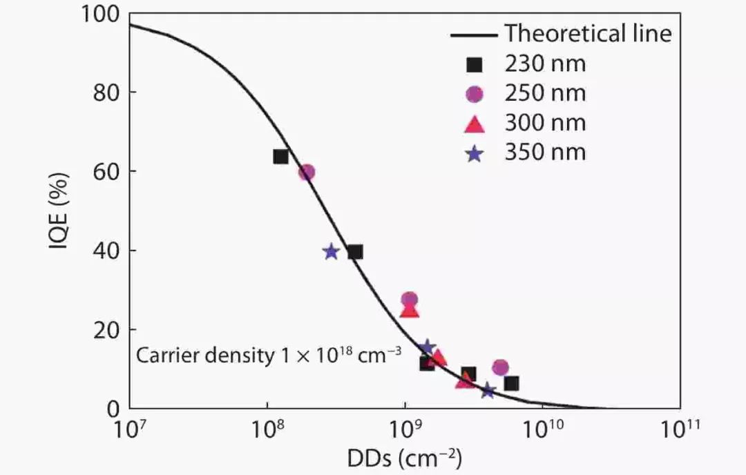
AlGaN-based materials own direct transition energy bands and wide bandgap and thus can be used in high-efficiency ultraviolet (UV) emitters. Compared with GaN-based blue and green LEDs and LDs, the efficiency of AlGaN-based UV LEDs and LDs is lower. Dislocations usually act as the nonradiative recombination center in AlGaN-based active devices, thus the quality of AlGaN is crucial to the device performance. Fig. 3 illustrates the relationship between the internal quantum efficiency (IQE) and the dislocation density (DD) in AlGaN multiple quantum wells (MQWs) underweak excitation with an excess carrier density of 1×1018cm-3[8]. It is difficult to obtain high-quality AlGaN material, and the crystalline quality of the material deteriorates with increasing Al content. The main reasons for the poor crystalline quality are a lack of lattice-matched substrates for growth and the presence of pre-reactions or parasitic reactions between the trimethylaluminum (TMAl) precursors and NH3 used in growth of the material.

Figure 3. IQE as a function of DD in an underlying layer under weak excitation with excess carrier density of 1 ×1018cm-3.
(2) Low light extraction efficiency
Due to the higher refractive index of nitride materials, the light emitted by quantum wells is totally reflected at the interface between DUV-LED and air. A large amount of light is confined inside the LED and absorbed by the epitaxial material, resulting in very low light extraction efficiency. N Lobo's simulations show that the light extraction efficiency of mirrorless and unpackaged flip-chip UV-LEDs is only 7%–9% level[9]. In addition, the luminescence of GaN-based visible light LEDs is mainly TE mode polarization, while in AlGaN-based UV-LEDs, as the Al composition increases and the wavelength decreases, the TE mode is converted to the TM mode. For the LEDs on the c-plane sapphire, the TE mode and the TM mode polarized light propagate vertically and horizontally, respectively, so the TE mode polarized light is easier to extract from the vertical direction than the TM mode polarized light, that is, TE mode has higher extraction efficiency than TM mold. Therefore, for AlGaN-based UV-LEDs, as the Al composition increases and the wavelength decreases, the TM mode polarization increases and the TE mode polarization decreases, which becomes another important factor for its low light extraction efficiency.
(3) P-type doping problem of AlGaN
High-conductivity AlGaN is required to realize high performance AlGaN-based UV devices. However, a problem that has persisted since the early 1990s and is becoming increasingly troublesome is the high resistivity of p-type GaN and AlGaN layers.The activation energy EA of the most commonly used acceptor dopant (Mg) in GaN is ~200 meV[10], several times the thermal energy kBT at room temperature (where kB is the Boltzmann constant, and T is temperature). The activation energy of acceptors increases with the band gap, reaching EA ~ 630 meV in AlN. Thus, the thermal activation of holes is highly inefficient at room temperature for GaN and becomes increasingly problematic for higher-band-gap AlGaN and AlN layers. As a result, injection of holes is a severe impediment for light-emitting devices in the UV and deep-UV spectral windows. High p-type resistance leads to excessive Joule heating of p-doped AlGaN layers for Al composition xAl ≥ 20%. Instead, p-GaN layers must be used and absorption losses incurred in the narrower-bandgap region. Furthermore, hole reflection and trapping at heterojunction valence-band offsets block hole injection into optically active AlGaN regions[1] and reduce the efficiency of such devices. An alternative strategy for efficient p-type doping and hole injection in wide-bandgap semiconductors is therefore highly desirable at this time.
In order to solve the above problems, the researchers have also made many efforts. For growing high-quality AlGaN film on sapphire substrates, a high-quality AlN film is mainly used as a template layer of AlGaN, so researchers used various methods to grow high-quality AlN films, such as pulse growth method, insertion of low-temperature buffer layer or two-dimensional materials such as graphene buffer layer and epitaxial lateral overgrowth (ELO) technology on patterned sapphire substrates (PSS)[11-13]. Meanwhile, drawing on the light extraction experience of GaN-based blue LEDs, on the basis of improving the transmittance of the p-type layer of the UV-LED and reducing the self-absorption of the epitaxial layer, techniques such as pattern substrate, surface roughening and electrode mirrors can further improve the LEE and EQE of UV-LEDs. SET Inc. used the transparent p-type cladding and contact layers to reduce the light absorption[14]. Mi et al. demonstrated a light extraction efficiency of more than 70% using nanowire DUV-LED[15].
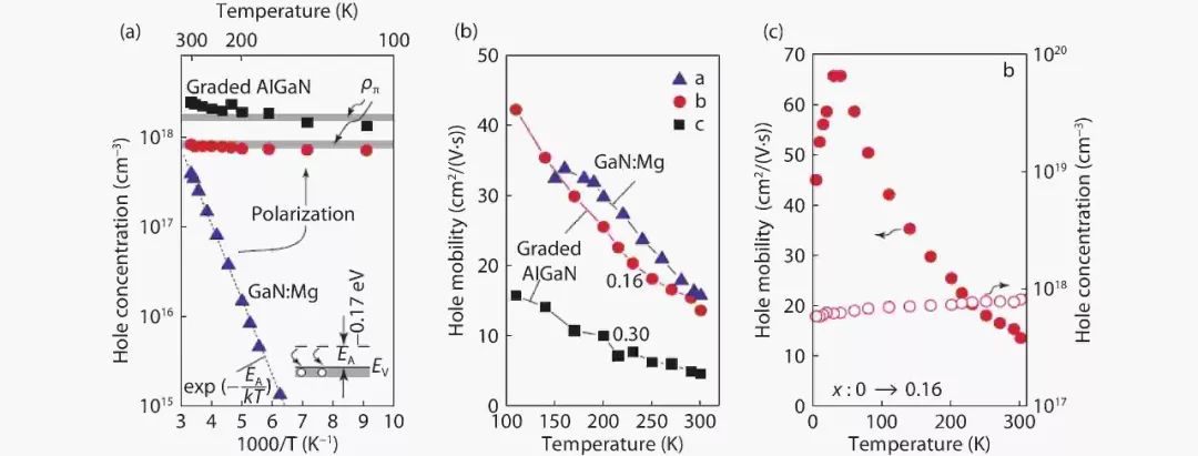
In addition, studies on p-doping of AlGaN have investigated common uniform Mg doping, Mg-δ doping, superlattice doping, co-doping, polarization induced doping and so on[16-18]. Simon et al. demonstrated high-efficiency p-type doping by ionizing acceptor dopants using the built-in electronic polarization in bulk uniaxial semiconductor crystals. Because the mobile hole gases are field-ionized, they are robust to thermal freeze out effects and lead to major improvements in p-type electrical conductivity. The new doping technique results in improved optical emission efficiency in prototype ultraviolet light-emitting diode structures (Fig. 4)[10].

Figure 4. Hall-effect temperature-dependent (a) hole concentration, (b) hole mobilities, and (c) hole concentration and mobility measured down to T = 4 K.
AlGaN-based DUV-LEDs with short operating wavelengths have been achieved, and these wavelengths have been extended to 222 nm for AlGaN/AlN MQW devices and 210 nm for AlN PIN homojunction devices. The improved performances of these LEDs have been achieved with EQEs of 20.3% at 275 nm. However, the EQEs of DUV-LEDs are still low when compared with those of GaN-based blue and green LEDs. There is also a considerable drop in efficiency, which is caused by high dislocation densities, low hole concentrations, and low LEEs for the AlGaN-based LEDs. Furthermore, the EQE also drops dramatically with decreasing wavelength, which is caused by deterioration in the AlGaN quality, the difficulty of p-type doping processes, and degradation of the optically polarized emission with increasing Al content. It is expected that high-efficiency DUV AlGaN-based LEDs will be realized by improving the quality and the p-type doping of AlGaN as well as optimizing the parameters of the AlGaN/AlN MQWs.
Due to the improvements in both AlGaN quality and p-type doping, UV stimulated emission has been achieved in AlGaN MQW LDs using electrical pumping at RT, with a shortest reported wavelength of 271 nm. At present, the development of UV AlGaN-based LDs is moving toward shorter wavelengths and low threshold voltage. However, many challenges still need to overcome to achieve high performance LDs of this type. First, the high densities of defects and dislocations in the active regions of these LDs will increase their internal losses, resulting in reduction of the EQE. Second, the difficulty involved in p-type doping of AlGaN will reduce the hole injection efficiency and increase the series resistance, which leads to an increased threshold and reduced efficiency for LDs operating under current injection conditions. Additionally, the difficulties faced in device fabrication processes such as etching, thinning, and cleaving will increase losses and reduce the efficiency of these LDs. In addition, suitable homoepitaxial substrates for AlGaN growth are not available at present. Therefore, appropriate substrates with high transparency and high electrical and thermal conductivities are required to improve the performance of these LDs. Furthermore, a suitable LD structure design is required to improve device efficiency. In conclusion, the low defect densities of bulk AlN substrates offer a promising strategy to enable fabrication of high-performance LDs.
References
[1] Khan A, Balakrishnan K, Katona T. Ultraviolet light-emitting diodes based on group three nitrides. Nat Photonics, 2008, 2, 77
[2] Li D, Jiang K, Sun X, et al. AlGaN photonics: recent advances in materials and ultraviolet devices. Adv Opt Photonics, 2018, 10, 43
[3] Takano T, Mino T, Sakai J, et al. Deep-ultraviolet light-emitting diodes with external quantum efficiency higher than 20% at 275 nm achieved by improving light-extraction efficiency. Appl Phys Express, 2017, 10, 031002
[4] Hodgkinson J, Tatam R P. Optical gas sensing: a review. Meas Sci Technol, 2013, 24, 012004
[5] Allaria E, Castronovo D, Cinquegrana P, et al. Two-stage seeded soft-X-ray free-electron laser. Nat Photonics, 2013, 7, 913
[6] Kneissl M, Seong T Y, Han J, et al. The emergence and prospects of deep-ultraviolet light-emitting diode technologies. Nat Photonics, 2019, 13, 233
[7] Zhang Z, Kushimoto M, Sakai T, et al. A 271.8 nm deep-ultraviolet laser diode for room temperature operation. Appl Phys Express, 2019, 12, 124003
[8] Ban K, Yamamoto J I, Takeda K, et al. Internal quantum efficiency of whole-composition-range AlGaN multi-quantum wells. Appl Phys Express, 2011, 4, 052101
[9] Kneissl M, Kolbe T, Chua C, et al. Advances in group III-nitride-based deep UV light-emitting diode technology. Semicond Sci Technol, 2011, 26, 014036
[10] Simon J, Protasenko V, Lian C, et al. Polarization-induced hole doping in wide-band-gap uniaxial semiconductor heterostructures. Sciences, 2009, 327, 60
[11] Chang H, Chen Z, Li W, et al. Graphene-assisted quasi-van der Waals epitaxy of AlN film for ultraviolet light emitting diodes on nano-patterned sapphire substrate. Appl Phys Lett, 2019, 114, 091107
[12] Hirayama H, Yatabe T, Noguchi N, et al. 231–261 nm AlGaN deep-ultraviolet light-emitting diodes fabricated on AlN multilayer buffers grown by ammonia pulse-flow method on sapphire. Appl Phys Lett, 2007, 91, 71901
[13] Tian W, Yan W Y, Dai J N, et al. Effect of growth temperature of an AlN intermediate layer on the growth mode of AlN grown by MOCVD. J Phys D, 2013, 46, 065303
[14] Shatalov M, Sun W, Lunev A, et al. AlGaN deep-ultraviolet light-emitting diodes with external quantum efficiency above 10%. Appl Phys Express, 2012, 5, 082101
[15] Djavid M, Mi Z. Ehancing the light extraction efficiency of AlGaN deep ultraviolet light emitting diodes by using nanowire structures. Appl Phys Lett, 2005, 108, 051102
[16] Jeon S R, Ren Z, Cui G, et al. Investigation of Mg doping in high-Al content p-type Al xGa1–xN (0.3 ≪ x ≪ 0.5). Appl Phys Lett, 2005, 86, 082107
[17] Nakarmi M L, Kim K H, Li J, et al. Enhanced p-type conduction in GaN and AlGaN by Mg-δ-doping. Appl Phys Lett, 2003, 82, 3041
[18] Zhong H X, Shi J J, Zhang M, et al. Improving p-type doping efficiency in Al0.83Ga0.17N alloy substituted by nanoscale (AlN)5/(GaN)1 superlattice with MgGa-ON δ-codoping: Role of O-atom in GaN monolayer. AIP Adv, 2015, 5, 227

Hideki Hirayama received his Ph.D. from Tokyo Institute of Technology in 1994. He joined RIKEN from 1994 and he was appointed Chief Scientist and Director of Quantum Optodevice Laboratory since 2012. His research interests include crystal growth of wide bandgap AlN-based nitride semiconductors and development of deep-UV emitters.
详情可阅Hideki Hirayama教授文章:
Research status and prospects of deep ultraviolet devices
Hideki Hirayama
J. Semicond. 2019, 40(12), 120301
doi: 10.1088/1674-4926/40/12/120301
《半导体学报》组织了一期“深紫外发光材料与器件”专题,并邀请中国科学院半导体研究所李晋闽研究员、北京大学王新强教授、中国科学院长春光学精密机械与物理研究所黎大兵研究员和中国科学院半导体研究所魏同波研究员共同担任特约编辑。该专题已于2019年第12期正式出版并可在线阅读,欢迎关注。

来源:半导体学报
编辑:拓跋猴儿


