IEDM: Automating DTCO for 3nm
编者按:在12月的IEDM上,TEL的Lars Liebmann提出了针对3nm及更高的工艺的设计工艺协同优化技术。如今的挑战在于,scaling不再仅基于工艺节点增长的增量的改变。设计工艺协同优化(DTCO)是一种更全面的进行工艺探索的方法。本文作者分享了他对这一问题的一些调研和思考。
At IEDM in December, Lars Liebmann of TEL presented Design Technology Co-Optimization for 3nm and Beyond. The challenge in designing a modern process is that scaling is no longer based on incremental change purely at the process level. Design Technology Co-Optimization (DTCO) is a way to do technology exploration more holistically. Some process feature can be proposed, and then the impact on cell libraries needs to be considered, and then the impact on placed-and-routed designs needs to be considered. This is obviously more complex and more expensive than just developing a PDK and then letting designers use it pretty much the same way as they used the prior node, especially if everything has to be done by hand.
DTCO was originally focused on design rule optimization, then it moved up to standard cell logic layout (in particular, reducing the number of metal tracks taken in the vertical dimension), and now encompasses the entire physical design flow since routability also depends critically on process features.
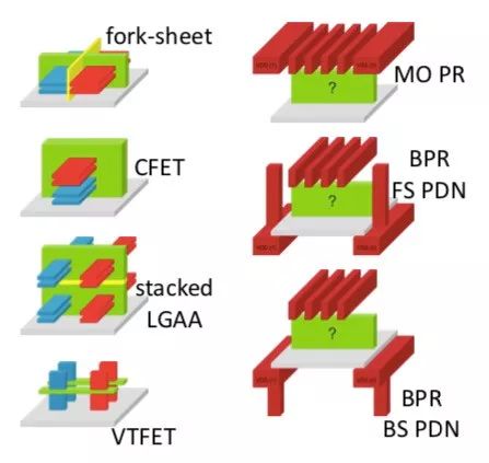
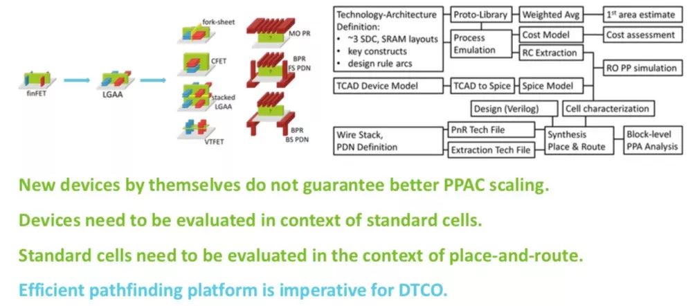
At 3nm, we have reached the end of just pitch scaling FinFETs. One big question is what comes next, such as gate-all-around, CFETs (stacking the N and P transistors), vertical gates, and so on. Another major consideration is buried power rail (BPR), or front-side power delivery, and other options that have a major impact on layout.
Lars pointed out that DTCO is different from design for manufacturability (DFM). It is three to five years out from high-volume manufacturing (HVM) and is used to understand the technology options. This allows the new requirements to be understood and costed, and the advantage in terms of area understood. A good example is buried power rail, putting the power rails into the silicon rather than keeping them in the interconnect. This obviously has major impact on the process itself, and the cost of a wafer, but also makes logic smaller. It is not immediately obvious whether that is a good tradeoff or not, and it is impossible to tell without building cell libraries and placing and routing some designs. DFM, on the other hand, is more like a year before HVM (and going on into the first year or two of the process) to tweak the process, identify yield detractors, and optimize the design.
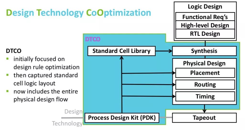
The traditional (old) way of doing process rollout was to develop a PDK, then ship it to early customers, design the standard cell libraries (and memories), build a place and route flow, and so on. But because of the lead times involved, there was minimal feedback into the process design from the results—once the process was designed it was effectively fixed. But increasingly restrictive rules forced negotiations between the different camps, the process people and the design people. In particular, process features are required to enable a reduction in the number of tracks in the standard cell libraries, since the amount of scaling from just shrinking the process is not enough.
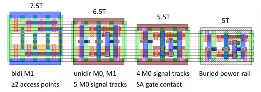
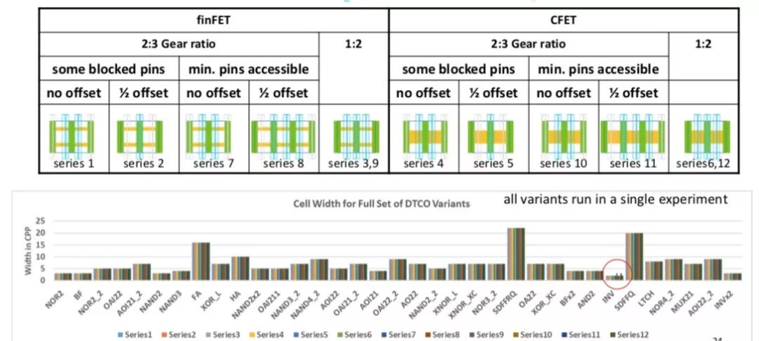
One side-effect of cell scaling is an increase in router congestion. In fact, Lars found that at 7nm the "7.5T library was so congested that the routed image is larger than 9T". This caused a shift in the way DTCO was used since you can't just trust guidelines for cell optimization, you have to actually do the experiments. However, you can't realistically replicate the entire product design for each potential process feature. There needs to be a streamlined technology prototyping that is more automated and iterative, as in the diagram below:
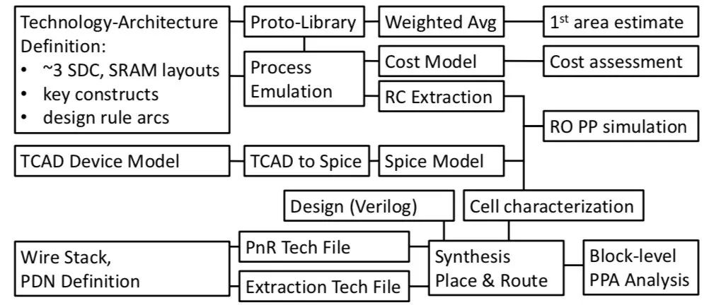
This then allows a series of different libraries to be created and experimented with, getting to a first estimate of a technology's scaling benefit and arriving at a go/no-go decision. Another feature of advanced nodes is that they may need to use higher conductivity metals such as cobalt or ruthenium, which have different costs. It is necessary to get down to this level of detail to see the true tradeoffs.
All these device options such as CFET, or GAA, or BPR, have a major impact on cell design and routability. Lars' final message was that devices by themselves do not guarantee better scaling, power, performance, and cost. They need to be evaluated in the context of standard cells. But even that is not enough, the standard cells need to be evaluated in the context of place and route. This is all too expensive to do for all the choices manually. An efficient pathfinding platform that automates much of the procedure is required.
看完有什么感想?
请留言参与讨论!