The solution for analyzing extreme ultraviolet photoresist
编者按:就先进技术节点(16nm节点以下)而言,CD的持续收缩以及如今许多新材料参与制造过程是需要着重考虑的因素。例如,极紫外光刻胶已经成为7nm及以下节点FinFET和未来GAA制造过程中最关键的材料之一。然而,据相关报道,EUV 光刻胶非常脆弱,对温度和例子高度敏感。
Atomic layer deposition (ALD) has attracted considerable attention in integrated circuit (IC) equipment industry in recent years. This is largely due to its superior properties, excellent coating conformity, and controllable coating thickness in single atomic layer, especially when compare to other coating systems.
Today, ALD has turned into a core technology in IC fabrication processes and its significance has become even more pronounced as a result of its advanced fabrication processes, including such modern solutions as 3D FinFET or even future gate-all-around (GAA), along with all other variants where precisely well-controlled coating thickness and thin film conformity in sub-nanometer level are in high demanded.
Apart from the above applications in IC fabrication, ALD can also be used for material analysis. A good example in this regard would be the transmission electron microscope (TEM), where by ALD is used to prepare a protection layer on top of areas of interest (AOI) before TEM lamella preparation. Here, it is well known that TEM lamellas are mainly prepared by focused ion beam (FIB). In order to protect AOI from ion bombardment during FIB milling, an external protection layer on top of AOI is indispensable. The material within this protection layer is generally carbon-based glues or metals, and the layer thickness varies from tens of nanometers up to about 500 nm. This protection layer can be coated on surface of AOIs by spin coaters or deposition systems in a vacuum chamber.
Now, depending on coating mechanisms, sample temperature and ion bombardment effects are two main factors that should be considered in order to prevent structures of AOI being altered or damaged during coating processes. For older technology nodes (bigger than 28 nm node), such coating can be easily achieved with wider preparation windows. This is because both the material and structure of AOI are relatively robust and stable. Generally speaking, coating with normal preparation conditions leads to no obvious structural changes or damages of the AOI when observing TEM results.
In terms of advanced technology nodes (below 16 nm node), continuous shrinkage of critical dimension (CD) along with the fact that many new materials are now involved in the fabrication processes are important factors to consider. For instance, extreme ultraviolet (EUV) photoresist (PR) has become one of the most crucial materials used in fabrication processes of 7 nm (and below) node FinFET and future GAA. However, it has been widely reported that EUV PR is extraordinarily fragile and highly sensitive to temperature and ion (both polarities). Damaged or deformed AOIs are expected to be found by traditional coating for older technology nodes, and pristine structures no longer exist for further analysis.
Coating conformity can also be problematic for structures with smaller CDs, such as vias or trenches, when using traditional methods. Extrinsic pinholes or bubbles are expected to be formed before vias or trenches being fully filled with the coating material. These unwanted artifacts could lead to possible difficulties in terms of preventing curtain effect during FIB milling and afterwards when it comes to TEM data interpretation.
To solve all of the above listed challenges, MSS proposes an innovative approach – utilizing a low-temperature vacuum ALD approach to prepare the protection layer on surface of AOIs. Because of its growth mechanism, ALD has an excellent coating conformity, so it is perfectly fitted for coating materials into vias, trenches, or other structures with smaller CDs.
When it comes to preventing damages from FIB milling and following TEM observation (high-energy electron damages), a thicker protection layer is preferred – at least 50 nm in thickness. This is because the thick protection layer is like a powerful armor and has a strong resistance to FIB milling and high-energy electron bombardment. Depending on surface properties of AOIs and analytic purposes, different protection materials can be prepared. Most importantly, despite varieties of protection materials, the sample temperature must always be kept at a low temperature throughout preparation – only a bit higher than room temperature, but certainly well below the one utilized in traditional coating systems. It is crucial, especially for EUV PR because all these steps have to ensure EUV PR stays intact throughout the whole analysis flow and precise results can be delivered.
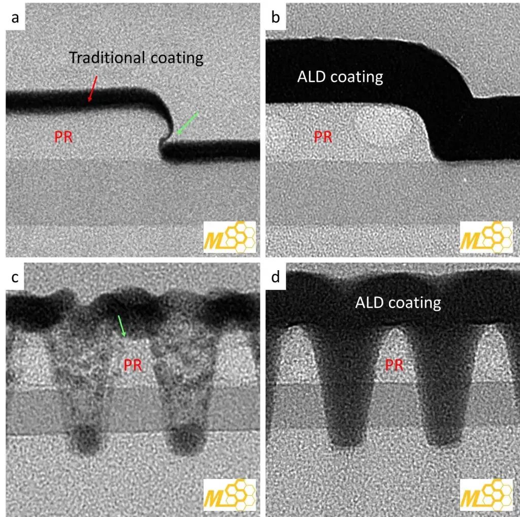
Figures 1a and 1c exhibit TEM images taken from two different PR samples. Their protection layers were all prepared by the traditional coating method. Poor coating conformity can be observed, especially in Fig. 1c. For comparison, an MSS low-temperature vacuum ALD has been utilized on another two samples with the same structures and materials as Figs. 1a and 1c. The TEM images are shown in Figs. 1b and 1d, respectively. From these TEM images, it is easy to see the PR structures prepared by the traditional coating have been damaged or modified, especially the areas marked by green arrows, with certain degree by comparing with the ones prepared by MSS ALD.

Figure 1. a-d TEM images of PR structures. Two different types of PR structures were utilized a, b and c, d. The protection layers in a and c were prepared by the traditional coating and those in b and d were prepared by MSS ALD coating. In a and c, obviously, the PR structures were damaged or altered by comparing with those in b and c, see the areas marked by green arrows.
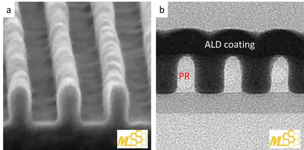
The question here now becomes how best to prove the low-temperature vacuum ALD coating has no effects on modifying PR structures as shown in Figs.1 a and 1c. To answer this question, we utilized one of our niche analyses, non-coating high-resolution SEM, to observe the pristine sample before ALD coating and the result is shown in Fig. 2a. The same sample was then coated with MSS ALD followed by FIB milling and TEM observation, and the result is shown in Fig. 2b. The fact that the PR structure shown in Fig. 2a is consistent with the one shown in Fig. 2b observed by TEM strongly suggests the PR structure does not need to be altered or damaged with our ALD preparation.

Figure 2. a High-resolution non-coating SEM image of the PR structure. b TEM image of the PR structure, the same structure as a and the protection layer was prepared by MSS ALD coating. By comparing with these two images, the PR structures stay the same after the ALD coating.
In conclusion, we have successfully demonstrated that MSS’s low-temperature vacuum ALD can be utilized for preparing a protection layer on EUV PR in order to prevent damages from FIB milling and TEM observation. Such sample protection can be applied to other fragile samples as well, and the concept can be extended to other purposes not only in material analysis but failure analysis or even surface analysis.
MSS’s theory on utilizing a low-temperature vacuum ALD for sample protection has been patented in 2020. We believe more and more samples will need such technology in the near future.
看完有什么感想?
请留言参与讨论!
