【Viewer】IBM宣布的2nm工艺实际如何?与Foundry的3nm比较如何?
IBM has announced the development of a 2nm process.
IBM Announcement
What was announced:
“2nm”
50 billion transistors in a “thumbnail” sized area later disclosed to be 150mm2 = 333 million transistors per millimeter (MTx/mm2).
44nm Contacted Poly Pitch (CPP) with 12nm gate length.
Gate All Around (GAA), there are several ways to do GAA, based on the cross sections IBM is using horizontal nanosheets (HNS).
The HNS stack is built over an oxide layer.
45% higher performance or 75% lower power versus the most advanced 7nm chips.
EUV patterning is used in the front end and allows the HNS sheet width to be varied between 15nm to 70nm. This is very useful to tune various areas of the circuit for low power or high performance and also for SRAM cells.
The sheets are 5nm thick and stacked three high.
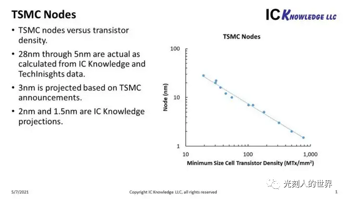
Is this really “2nm” as claimed by IBM? The current leader in production process technology is TSMC. We have plotted TSMC node names versus transistor density and fitted a curve with a 0.99 R2 value, see figure 1.

Figure 1. TSMC Equivalent Nodes.
Using the curve fit we can convert transistor density to a TSMC Equivalent Node (TEN). Using curve fit we get a TEN of 2.9nm for the IBM announced 333MTx/mm2. In our opinion this makes the announcement a 3nm node, not a 2nm node.
To compare the IBM announcement in more detail to previously announced 3nm processes and projected 2nm processes we need to make some estimates.
We know the CPP is 44nm from the announcement.
We are assuming a Single Diffusion Break (SDB) that would result in the densest process.
Looking at the cross section that was in the announcement, we do not see Buried Power Rails (BPR), BPR is required to reduce HNS track height down to 5.0, so we assume 6.0 for the process.
To get to 333MTx/mm2 the Minimum Metal Pitch must be 18nm, a very aggressive value likely requiring EUV multipatterning.
IBM 2nm Versus Foundry 3nm
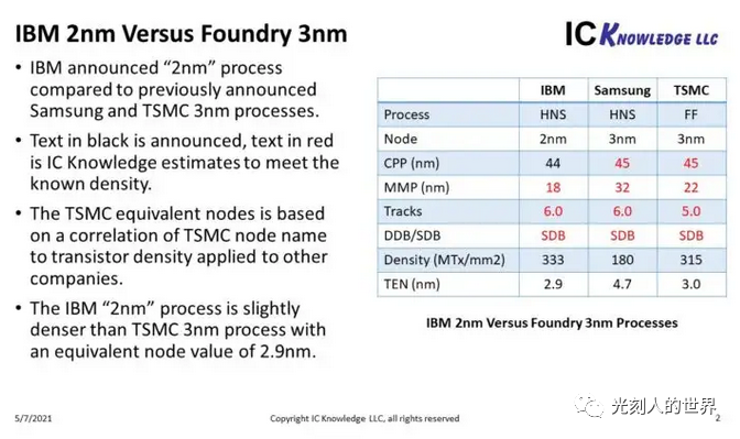
Figure 2 compares the IBM 2nm devise to our estimates for Samsung and TSMC 3nm processes. We know Samsung is also doing a HNS and TSMC is staying with a FinFET at 3nm. Samsung and TSMC have both announced density improvements for their 3nm processes versus their 5nm processes so we have known transistor density for all three companies and can compute TEN for all three. As previously noted, IBM’s TEN is 2.9, we now see Samsung’s TEN is 4.7 and TSMC’s TEN is 3.0 again reinforcing that IBM 2nm is like TSMC 3nm and Samsung is lagging TSMC.
The numbers in red in figure 2 are estimated to achieve the announced densities, We assume SDB for all companies. TSMC has the smallest track height because a FinFET can have a 5.0 track height without BPR, but HNS needs BPR to reach 5.0 in BPR isn’t ready yet.

Figure 2. IBM 2nm Versus Foundry 3nm.
IBM 2nm Versus Foundry 2nm
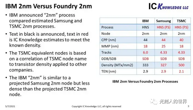
We have also projected Samsung and TSMC 2nm processes in figure 3. We are projecting that both companies will use BPR (BPR is not ready yet but likely will be when Samsung and TSMC introduce 2nm around 2023/2024). We also assume that Samsung and TSMC will utilize a forksheet NHS (HNS (FS) architecture to reach a 4.33 track height relaxing some of the other shrink requirements. We have then projected out CPP and MMP based on the company’s recent shrink trends.

Figure 3. IBM 2nm Versus Foundry 2nm.
Power and Performance
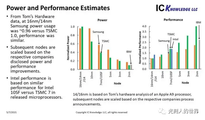
At ISS this year I estimated relative power and performance for Samsung and TSMC by node with some additional Intel performance data. The trend by node is based on the companies announced power and performance scaling estimates versus available comparisons at 14nm/16nm. For more information see the ISS article here.
Since IBM compared their power and performance improvements to leading 7nm performance I can place the IBM power and performance on the same trend plots I previously presented, see figure 4.

Figure 4. Power and Performance (estimates).
IBM’s use of HNS yields a significant reduction in power and makes their 2nm process more power efficient than Samsung or TSMC’s 3nm process, although we believe once TSMC adopts HNS at 2nm they will be as good or better than IBM for power. For performance we estimate that TSMC’s 3nm process will outperform the IBM 2nm process.
As discussed in the ISS article these trends are only estimates and are based on a lot of assumptions but are the best projections we can put together.
Conclusion
After analyzing the IBM announcement, we believe their “2nm” process is more like a 3nm TSMC process from a density perspective with better power but inferior performance. The IBM announcement is impressive but is a research device that only has a clear benefit versus TSMC’s 3nm process for power and TSMC 3nm will be in risk starts later this year and production next year.
We further believe that TSMC will have the leadership position in density, power, and performance at 2nm when their process enters production around 2023/2024.
看完有什么感想?
请留言参与讨论!
