来源:内容由半导体行业观察(ID:icbank)编译自「anandtech」,谢谢。
半导体行业观察最有深度的半导体新媒体,实讯、专业、原创、深度,50万半导体精英关注!专注观察全球半导体最新资讯、技术前沿、发展趋势。《摩尔精英》《中国集成电路》共同出品,欢迎订阅摩尔旗下公众号:摩尔精英MooreElite、摩尔芯闻、摩尔芯球
2175篇原创内容
公众号
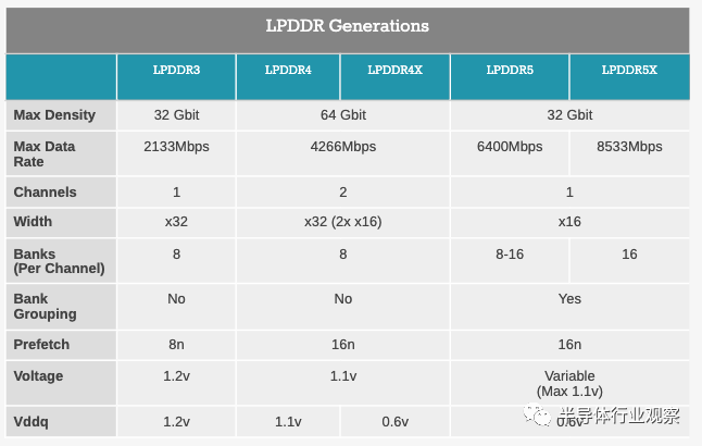
JEDEC 和 JC-42.6 低功耗存储器小组委员会已宣布发布新的 JESD209-5B 标准,该标准现在包括对 LPDDR5 的改进,以及以新 的LPDDR5X 形式出现的,对现有标准的扩展。新的 LPDDR5X 标准是 LPDDR5 的演进步骤,将可能的数据速率从 6400Mbps 进一步提高了 33% 到 8533Mbps。早在 2020 年,该行业就首次转向LPDDR5 内存标准,第一代 SoC和内存模块的运行速度为 5500Mbps,在最近的 2021 年旗舰设备中升级到了 6400Mbps。随着 IP 供应商和 DRAM 制造商的 LPDDR5 产品成熟,越来越需要寻找 LPDDR5 标准的进一步更新,因为我们在当前一代实施中基本上达到了标准的最大数据速率。虽然我们目前无法访问官方文档来详细说明确切的更改,但早在 2 月份,Cadence 就撰写了关于 LP5X 相对于 LP5 的新改进的文章:为了在高速双列系统中提高 READ SI 性能,Lpddr5X 设备支持统一( Unified ) NT-ODT 行为已被定义。统一 NT-ODT 是所有 LPDDR5X 设备的要求;为了支持 Lpddr5X 的高数据速率,我们需要一种补偿传输损失的方法。这是通过定义pre-emphasis功能来实现的。Lpddr5X 器件对每个低字节/高字节通道编程都有上拉或下拉pre-emphasis;Rx Offset Calibration Training - LPDDR5X SDRAM 提供 Offset Calibration Training 用于调整 DQ Rx Offset 和 Offset Calibration Training 建议用于每个上电和初始化训练序列以应对 SDRAM 操作条件变化;扩展延迟- LPDDR5X SDRAM 设备支持扩展读取、写入、nWR、ODTLon 和 ODTLoff 延迟值,以解决对存储器阵列进行数据访问所需的更长周期数。WCK2CK 同步交流参数也得到扩展;LPDDR5X SDRAM 器件支持每引脚控制的决策反馈均衡:DFE。这包括新的模式寄存器 70/71/72/73/74;937.5 /1066.5MHz 的新LPDDR5X SDRAM 设备特定时钟 AC时序和 3750/4266.5MHz 的写入时钟 AC 时序;新的模式寄存器字段或使用现有字段的附加条件已添加到 LPDDR5X 器件的多个模式寄存器中。已更改 MR 的一些示例是 MR0、MR1、MR2、MR13、MR15、MR41、MR58、MR69 等;LPDDR5X SDRAM 器件不支持 8 Bank操作模式。8 Bank 模式不提供 16B 和 BG 模式具有的更多 bank 交错资源和高速核心操作时序的架构优势。它特别限制了高速 LPDDR5X 设备支持领先的 JEDEC 放弃对 LPDDR5X 的 8 Bank 模式支持;简而言之,新标准涵盖了对内存标准架构和操作模式的更深入调整,以实现更高的数据速率。对于最终使用 8533Mbps 内存的移动 SoC,峰值理论可用带宽将从 51.2GB/s 增长到 68.26GB/s,允许未来的设计进一步提高 CPU 和 GPU 性能。需要注意的是,我们对新 LP5X 标准的能效改进知之甚少,因此我认为我们将依靠 DRAM 供应商通过更先进的制造节点来提高能效,从而将总用电量保持在设备在检查。我估计我们将在 2022 年末或 2023 年的 SoC 中看到 LPDDR5X。
JEDEC and the JC-42.6 Subcommittee for Low Power Memories has announced the publication of the new JESD209-5B standard which now includes improvements to LPDDR5, as well as an extension for the standard in the form of new LPDDR5X.The new LPDDR5X standard is an evolutionary step over LPDDR5, further increasing the data rates possible by 33% from 6400Mbps to 8533Mbps.The industry had first shifted over to the LPDDR5 memory standard back in 2020, with the first generation SoCs and memory modules running at a speed of 5500Mbps which had gotten an upgrade to 6400Mbps speeds in recent 2021 flagship devices.As IP vendors and DRAM manufacturers have matured their LPDDR5 products, there’s an increasing need to look for further updates to the LPDDR5 standard as we’ve essentially reached the maximum data rates of the standard in current generation implementations.While we currently don’t have access to the official documentation to detail the exact changes, back in February Cadence had written more extensively about the new improvements in LP5X over LP5:To Improve READ SI performance in the dual rank system at high speeds that Lpddr5X devices support a Unified NT-ODT Behavior has been defined. Unified NT-ODT is a requirement for all LPDDR5X devicesTo support high data rates for Lpddr5X, we need a way to compensate for transmission loss. This has been achieved by defining the pre-emphasis function. Lpddr5X devices have pull up or down pre-emphasis for each of the lower/upper byte lane programming.Rx Offset Calibration Training - LPDDR5X SDRAM provides Offset Calibration Training for adjusting DQ Rx offset and Offset Calibration Training is recommended for every power-up and initialization training sequence to cope with the SDRAM operating condition changeExtended Latencies - LPDDR5X SDRAM devices support extended Read, Write, nWR, ODTLon and ODTLoff Latency Values to account for longer number of cycle it takes to do the data access to memory array. WCK2CK Sync AC Parameters are also extended.LPDDR5X SDRAM Devices support Per-pin controlled Decision Feedback Equalization: DFE. This includes new Mode Registers 70/71/72/73/74.New LPDDR5X SDRAM Device specific Clock AC Timings for 937.5/1066.5MHz and Write Clock AC Timings for 3750/4266.5MHz.New Mode register fields or additional conditions on the use of existing fields have been added to several Mode registers for LPDDR5X devices. Some of the examples of changed MR are MR0, MR1, MR2, MR13, MR15, MR41, MR58, MR69, etc.LPDDR5X SDRAM devices do not support 8 Bank Mode of operations. 8 Bank Mode doesn’t offer the architectural benefit of more bank interleaving resources and core operation timings at high speed that 16B and BG Mode have. It is specially limiting for high speed LPDDR5X devices support leading JEDEC to drop 8 Bank Mode support for LPDDR5X.In short, the new standard covers deeper tweaks to the architecture and operating mode of the memory standard to achieve higher data-rates.For eventual mobile SoCs using 8533Mbps memory, the peak theoretical available bandwidth would grow from 51.2GB/s to 68.26GB/s, allowing future designs to further increase CPU and GPU performances. It’s to be noted, that we haven’t heard much about power efficiency improvements of the new LP5X standard, so I assume that we’ll be relying on DRAM vendors to improve power efficiency via more advanced manufacturing nodes to keep total power usage inside of devices in check.I estimate we’ll be seeing LPDDR5X in future late 2022 or 2023 SoCs.
★ 点击文末【阅读原文】,可查看本文原文链接!
摩尔芯闻您的半导体行业内参,每日精选8条全球半导体产业重大新闻解读,一天只花10分钟,享受CEO的定制内容服务。与30万半导体精英一起,订阅您的私家芯闻秘书!欢迎订阅摩尔精英旗下更多公众号:摩尔精英、半导体行业观察、摩尔App
237篇原创内容
公众号
*免责声明:本文由作者原创。文章内容系作者个人观点,半导体行业观察转载仅为了传达一种不同的观点,不代表半导体行业观察对该观点赞同或支持,如果有任何异议,欢迎联系半导体行业观察。
今天是《半导体行业观察》为您分享的第2751内容,欢迎关注。
『半导体第一垂直媒体』
实时 专业 原创 深度
识别二维码,回复下方关键词,阅读更多
晶圆|集成电路|设备|汽车芯片|存储|MLCC|英伟达|模拟芯片
回复 投稿,看《如何成为“半导体行业观察”的一员 》
回复 搜索,还能轻松找到其他你感兴趣的文章!